- Home
- Blog
- Tech Popularization
- Anbon Semiconductor Debuts at the 2026 Japan Electronics Show
Anbon Semiconductor Debuts at the 2026 Japan Electronics Show
Limitations of the first-generation architecture and directions for AI-driven innovation
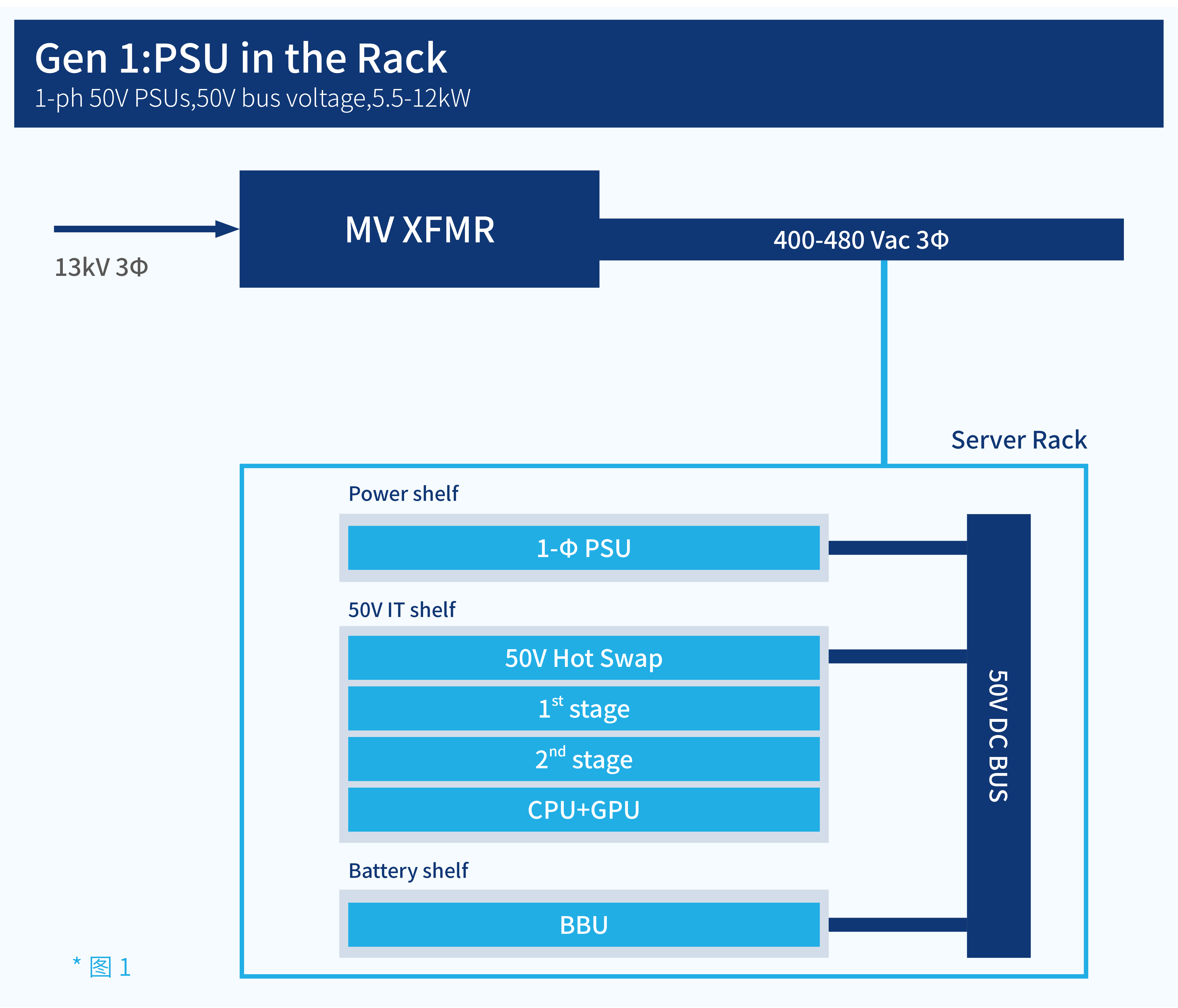
The two images below show the development of server rack architecture from the first generation to the second generation. The one on the left shows the first-generation architecture, where each power rack is powered by a three-phase input and comes with multiple power supply units (PSUs); each PSU is powered by a single-phase input. The rack outputs DC voltage (for example, 50V) to the bus, and the bus is connected to both the rack and the battery rack. The current rack architecture uses 5.5kW ORv3-HPR PSUs, but PSUs up to 12kW can also be used for higher power. For example, a rack with 4 modules of 12kW PSUs can provide a total rack power of 288kW.
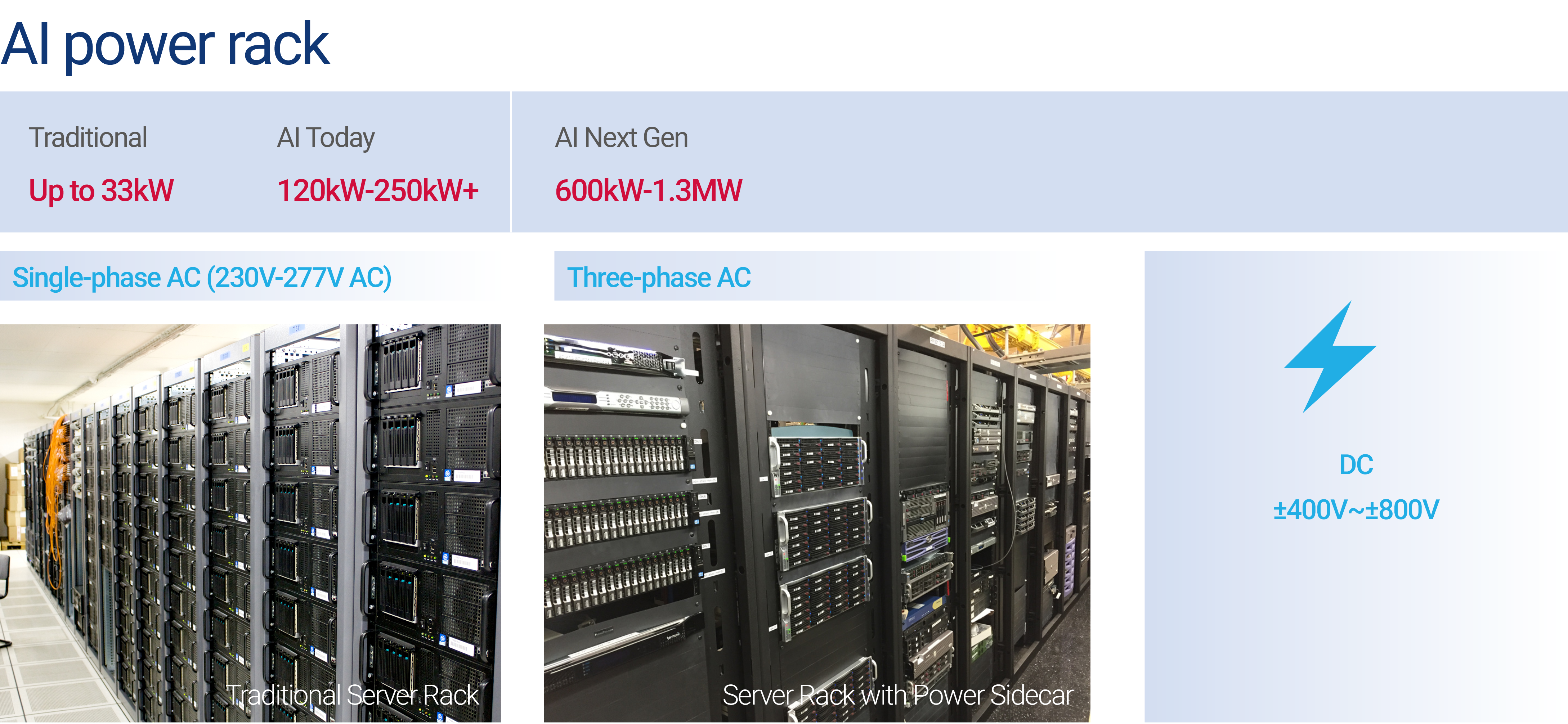
The development trend of artificial intelligence requires upgrades to power supply systems (PSU) and rack power. When the rack power exceeds 250 kW, space constraints make it difficult to integrate all power and computing components within the same rack, so separating the power components from the computing rack becomes logical.
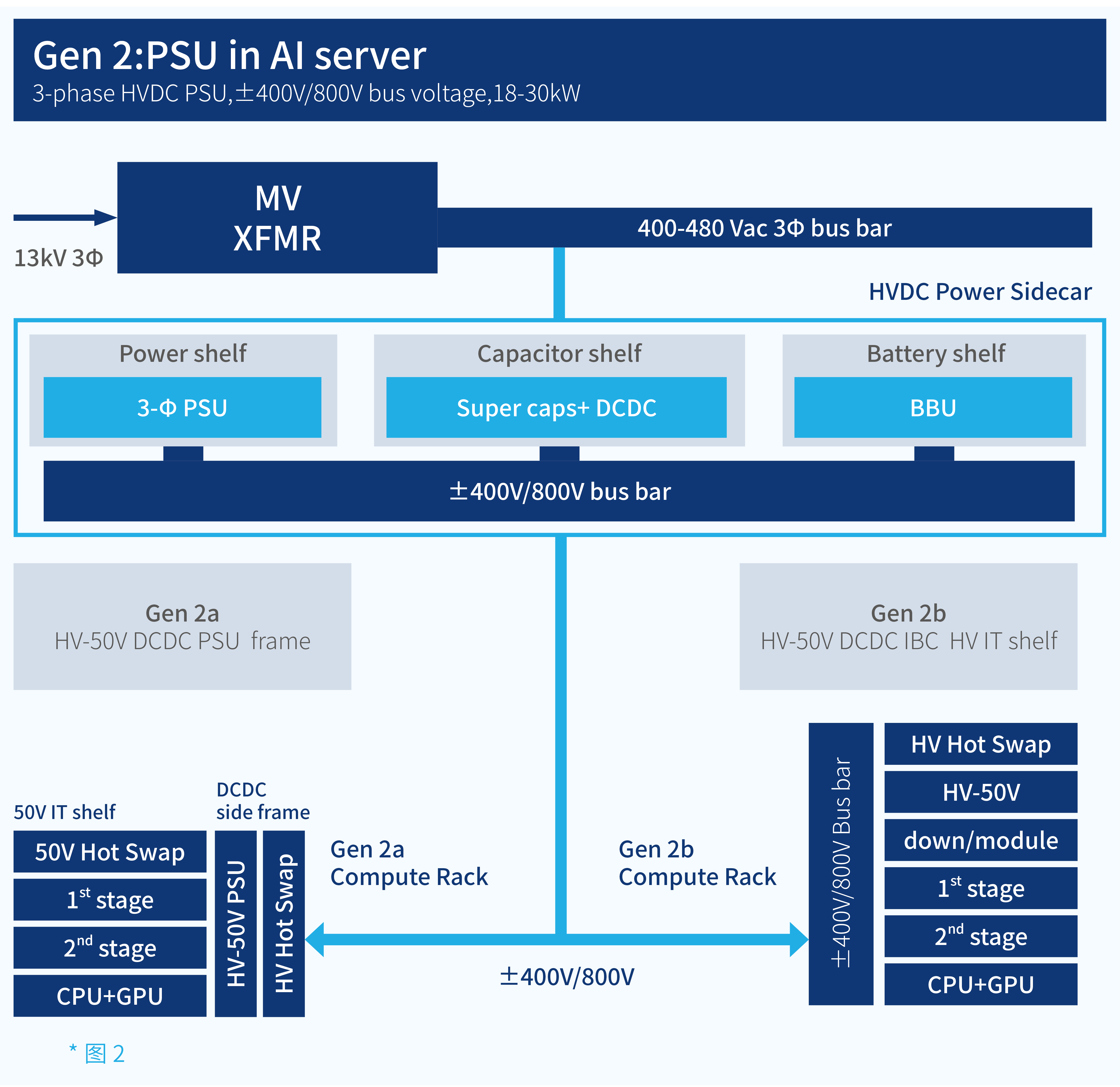
Figure 2 shows the second-generation solution, where the power-side cabin contains the PSU, battery backup unit (BBU), and capacitor bank unit (CBU). The PSU can reach up to 30 kW, with three-phase AC input and high-voltage DC (HVDC) output. The power-side cabin can be scaled up to 1 MW, freeing up more space in the computing rack to host additional computing power. The HVDC output from the power-side cabin connects to the computing rack via cables, which requires an extra step to step down HVDC voltage to 50 volts.
Figure 2 shows two implementation schemes: second-generation a and second-generation b, representing different ways of converting HVDC to 50V. Second-generation a is based on the existing 50V server tray, integrating the HVDC-to-50V conversion on the side of the rack in a DC-DC rack (the 'pocket' on the side frame). This layout takes advantage of the existing 50V server infrastructure while speeding up and simplifying the deployment of the HVDC-side cabin architecture. The later second-generation b scheme modularizes the HVDC-to-50V conversion into an intermediate bus converter (IBC) or buck converter solution, directly integrated inside the server tray. ...
Breakthroughs and Plans for Three-Phase High-Voltage DC Topology
Second-Generation AI Power Supply: A three-phase high-voltage DC architecture achieves maximum power output (about 18-30 kW), with ±400/800V output voltage, and supports 400/480V AC three-phase power. To further boost rack power, the second-generation AI power supply will adopt a more groundbreaking rack architecture, specifically including: upgrading the power input from single-phase to three-phase to improve density and cost efficiency; increasing the power output voltage from 50V to ±400/800V to reduce bus current, losses, and costs.
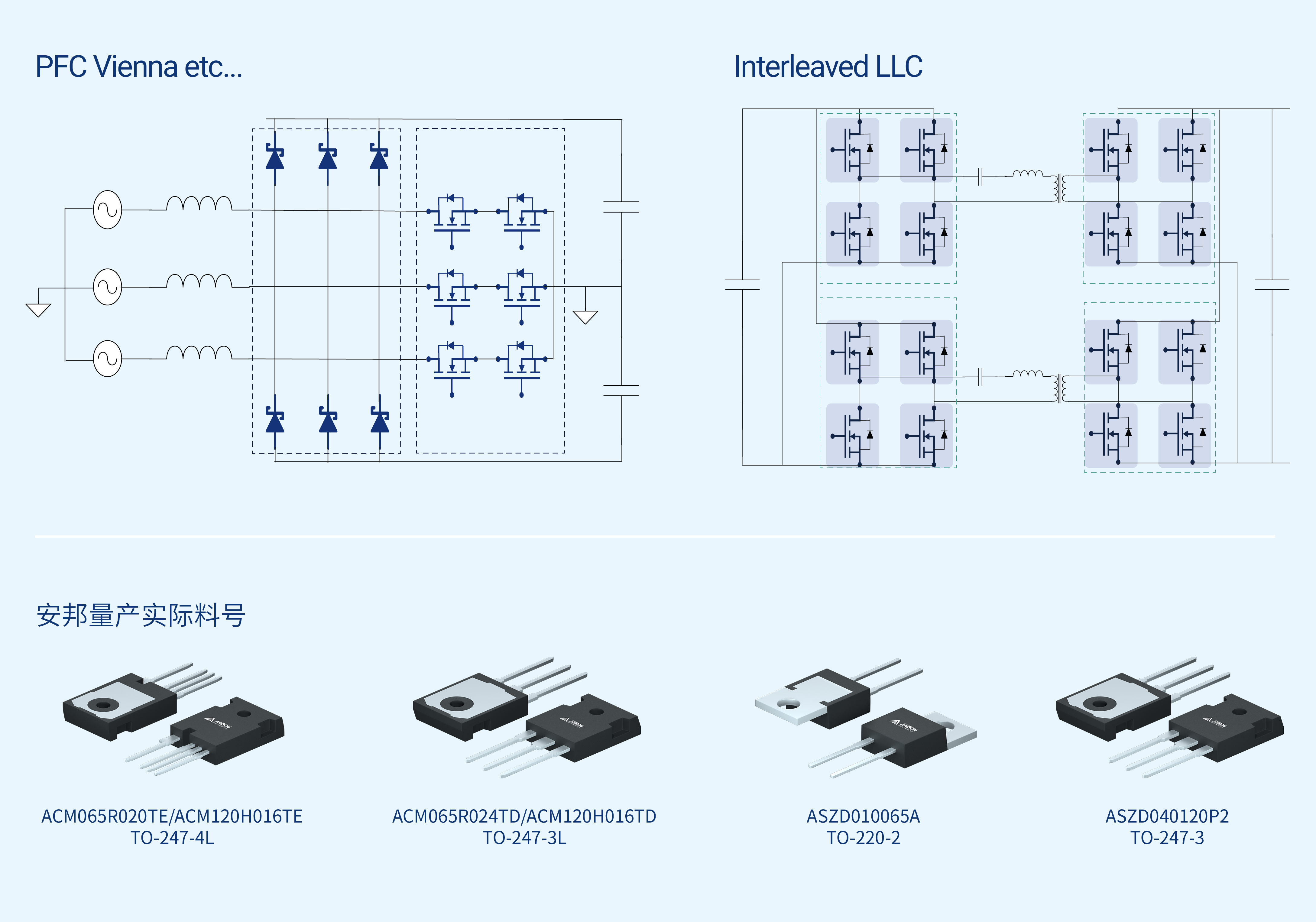
The image shows a typical topology example of a second-generation power supply, including recommended devices and technical solutions for three-phase input and high-voltage DC output. The Power Factor Correction (PFC) stage uses a Vienna converter, which is a widely popular topology in three-phase PFC applications. Its main advantage is that, with a split-voltage bus, it can use 650V back-to-back silicon carbide (SiC) FETs, and the input side uses 1200V SiC diodes, combining simplicity in structure with cost benefits. Another option is a T-type topology, which improves efficiency by replacing the input-side diodes with 1200V SiC FETs, reducing conduction losses. The LLC (inductor-inductor-capacitor) stage can be configured in two interleaved (parallel) stages or two cascaded (series) stages. In the interleaved configuration, each LLC stage is connected to the full bus voltage of around 860V, with 1200V SiC FETs on the primary side.
Another option is a PFC output with split capacitors, with the two LLC stages connected in series, using 650V GaN or SiC transistors on the primary side. Whether it's a series or parallel LLC structure, the two LLC secondary sides can be connected in parallel: synchronous rectifiers can use 650V SiC, ORing FETs for 400V output, and 1200V SiC MOSFETs for 800V output.
Key component empowerment
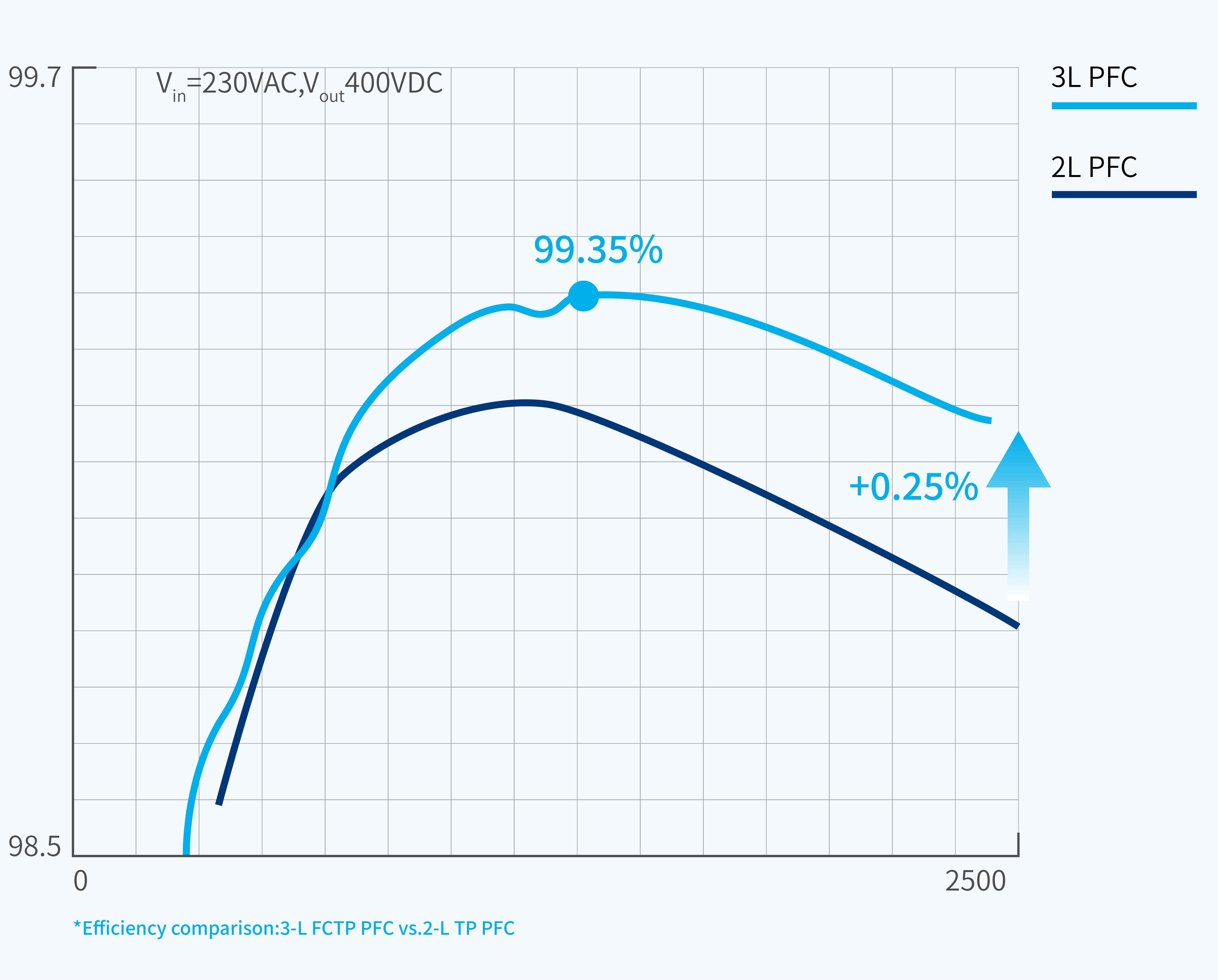
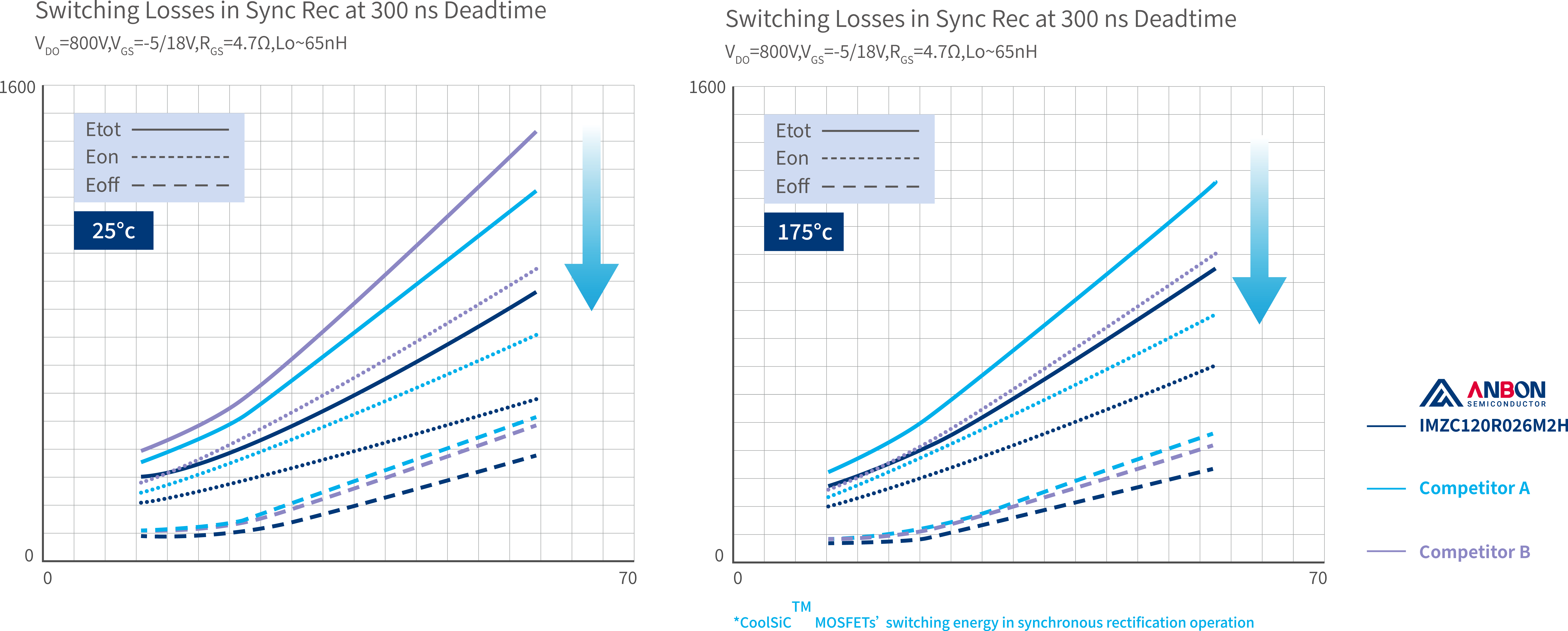
The 650V SiC MOSFET plays a key role in the back-to-back switching during the PFC stage of the inverter, while the 1200V SiC MOSFET/diode is used for the input bridge of the Vienna/T-type PFC. Depending on the LLC configuration and output voltage, the DC-DC stage requires 650V or 1200V SiC MOSFETs to drive the main-side switches and the secondary-side synchronous rectifiers. The attached figure shows benchmark tests of switching energy for SiC MOSFETs during synchronous rectification at room temperature and high temperature compared to competitors. It clearly shows a significant reduction in switching energy, which greatly reduces losses in the PFC and LLC stages of three-phase high-voltage DC power supplies.

Anbon Team
Responsible for sharing Anbon’s brand vision, product applications, and industry insights. By transforming technical knowledge into clear and accessible content, the Anbon Editor helps readers stay informed on market trends while bridging innovation with real-world applications and conveying Anbon’s core values.